X
In 1949, it took ENIAC (Electronic Numerical Integrator And Computer) 70 hours to calculate the value of Pi up to 2037 digits. Now, the smartphone in your hand can do the same task in 0.01 Seconds. The miraculous growth in speed was made possible by a tiny device inside electronic gadgets called a transistor. More specifically a type of transistor called MOSFET. MOSFET is an electrically driven switch, which allows and prevents a flow of current, without any mechanical moving parts. The MOSFET stands for Metal Oxide Semiconductor Filed Effect Transistor(refer Fig 1).
In MOSFET, the MOS part is related to the structure of the transistor, while the FET part is related to how it works. It is also known as IGFET (Insulated Gate Field Effect Transistor). The following image we have shown is a practical MOSFET. But in the digital world, the size of MOSFET is too small (in nm) that billions of them can be fabricated on a single chip.
There are two basic types of MOSFET:
1. Enhancement - MOSFET
2. Depletion - MOSFET
Here we are explaining most popular type, Enhancement-MOSFET or E-MOSFET.
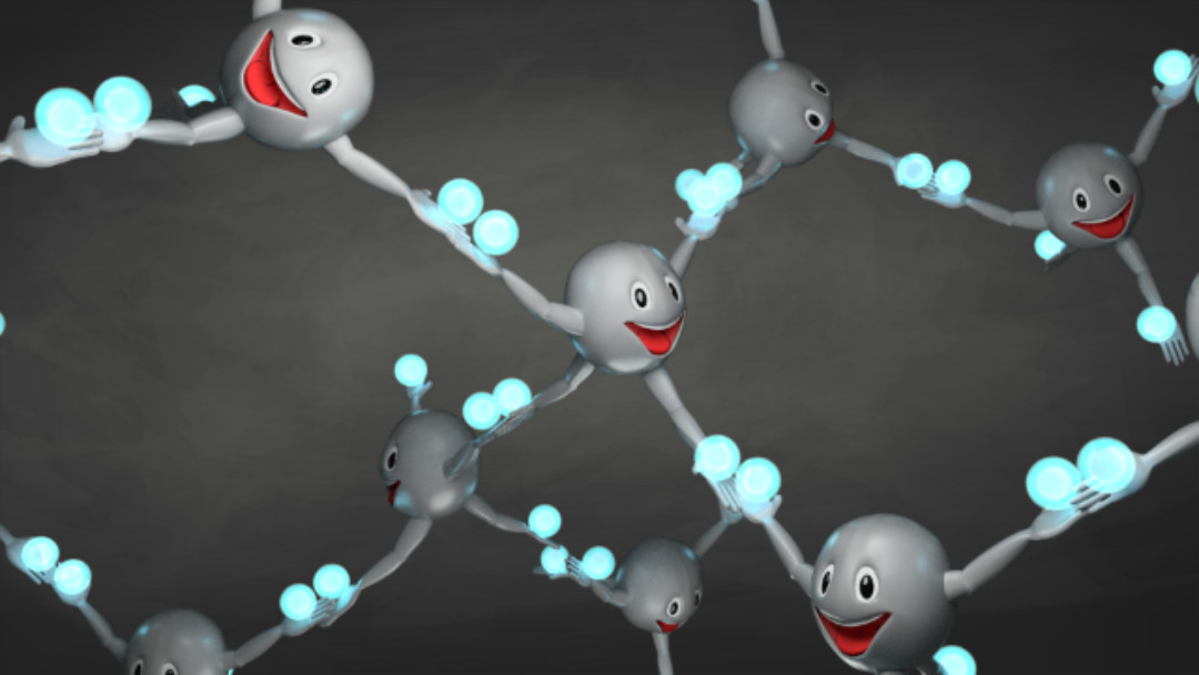
Like any other conventional transistor, A MOSFET is also made from a semiconductor material such as silicon. In its pure form, a semiconductor has very low electrical conductivity. However, when you introduce a controlled amount of impurities into the semiconductor material, its conductivity increases sharply. This procedure of adding impurities is called doping and the impurity is called dopant.
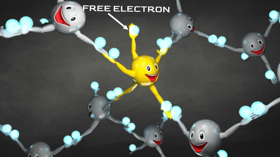
Pure silicon does not have any free electrons (refer Fig 2a ), and because of this its conductivity is very low; however, when you inject an impurity, which has extra electrons, into the silicon, the conductivity of the resultant material increases dramatically. This is known as N-type doping (refer Fig 2b). We can also add impurities with fewer electrons, which will also increase the conductivity of pure silicon. This is known as P-type doping (refer Fig 2c).
When the concentration of the impurity is lower (approx. one dopant atom is added per 100 million atoms), the doping is said to be low or light. On the other hand, if it is higher, the doping is referred to as high or heavy. Now, let's get back to the workings of MOSFETs. If you dope a silicon wafer with two highly doped n region as shown in the figure, you will get the basic structure of a MOSFET (refer Fig 3). It is interesting to note that, even in the P region, there are very few free electrons that are capable of conducting electricity. We call them minority carriers. Later we will see why the minority carriers are significant in the MOSFET.
Whenever a P-N junction is formed, the excess electrons in the N region have a tendency to occupy the holes in the P region. This means that the PN junction boundary naturally becomes free of holes or free electrons. This region is called a depletion region. The same phenomenon also happens in the P-N junction of the MOSFET (refer Fig 4).
Now let's connect a power cell across the MOSFET as shown in the figure (refer Fig 5). On the right-hand side P-N junction, the electrons are attracted to the positive side of the cell and the holes are moved away. In short, the depletion region width on the right-hand side is increased due to the power source. This means that there won’t be any electron flow through the MOSFET.
In short with this simple arrangement the MOSFET will not work. Let’s see how it is possible to have an electron flow in the MOSFET using a simple technique. To do this we first need to understand the workings of the capacitor.
Inside the capacitor, you can see two parallel metal plates separated by an insulator (refer Fig 6). When you apply a DC power source across these, the positive terminal of the cell attracts electrons in the metal plate and these electrons are accumulated on the other metal plate. This accumulation of charge creates an electric field between the plates.
Let’s replace one plate of the capacitor with the P type substrate of the MOSFET. If you connect a power source across the MOSFET as shown, just as in a capacitor the electrons will leave the metal plate. In a MOSFET these electrons will be dispersed into the P-substrate (refer Fig 7).
The positive charge generated on the metal plate, due to the electron displacement, will generate an electric field as shown. Due to the presence of electric field the MOSFET possess FET; Field Effect Transistor in its name.
Remember, there are some free electrons even in the P-type region. The electric field produced by the capacitive action will attract the electrons to the top. We will assume the electric field generated is quite strong. Some electrons were recombined with the holes, and the top region becomes overcrowded with electrons after all the holes there are filled. Just below this region, all the holes were filled but there were no free electrons either. This region has become a new depletion region. This process essentially breaks the depletion region barrier and a channel for the flow of electrons is created (refer Fig 8). If we apply a second power source as we did at the beginning the electrons easily flow towards the metal plate. This is the way a MOSFET turns to the ON state (refer Fig 9).
You can easily correlate the naming of the transistor terminals; Source, Drain and Gate with the nature of the electron flow. If the applied voltage is not sufficient enough or less than the threshold voltage, the electric field will be weak and there won’t be a channel formation and hence no electron flows. Thus just by controlling the GATE voltage, we will be able to turn the MOSFET ON and OFF. Due to this ability to change conductivity with the amount of applied voltage at the gate, the MOSFET is also known as Voltage Controlled Device. The threshold voltage of MOSFET mainly depends on the thickness of the oxide layer.
In MOSFET both the source and drain must be at higher or equal potential than the substrate to stop an unwanted electron flow. Since drain voltage is always greater than the substrate voltage, so we don't consider the drain-substrate side. Whereas in the source side, this electron flow is stopped by keeping source and substrate at the same potential. That's why in MOSFET, the source is always connected to the substrate.
Example:
Consider the heat-based fire alarm circuit as shown in the figure (refer Fig 10). This circuitry consists of a Thermistor, a buzzer, a MOSFET and some other passive components. The thermistor in the circuit decreases its resistance with an increase in temperature. Initially, at room temperature, the voltage at the GATE is low due to the high thermistor resistance, and that is not sufficient to turn ON the MOSFET. If the temperature increases, the thermistor’s resistance decreases, this will lead to a high GATE voltage, which then turns ON the MOSFET and the alarm.
MOSFETs open the door to digital memory and digital processing.
MOSFETs combine together to form the basic memory element of a static RAM.
At the lowest level MOSFETs are interconnected to form logic gates.
At the next level, the gates are combined to form processing units that perform thousands of logical and arithmetical operations.
1. Unlike BJTs, MOSFET have a scalable nature, so that millions of MOSFET can be fabricated on the single wafer.
2. A BJT wastes a small part of its main current when it’s switched ON; such power wastage is not there in MOSFETs.
3. The other advantage of a MOSFET is that it is a unipolar device means; it only operates with one type of charge carrier, be it a hole or an electron, so it is less noisy.
Thank you for reading!
All Rights Reserved | Copyright © 2022 | Lesics Engineers Pvt. Ltd.